
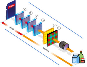
Every photograph you have ever taken—every portrait, landscape, and candid moment—begins with a single component: the image sensor. This tiny silicon chip is the digital equivalent of film, converting light into the electrical signals that become your photos and videos. And in 2026, camera sensor technology is undergoing its most dramatic transformation in decades.
The global image sensor market is projected to reach $32.5 billion in 2026, with expectations to grow to $68.7 billion by 2034. CMOS image sensors alone are forecast to grow from $24.58 billion in 2025 to $26.31 billion in 2026, reaching $36.96 billion by 2031. This explosive growth reflects a simple truth: sensor technology is the foundation of modern visual culture.
But what exactly is changing? And why should you care?
Whether you are a professional photographer, a smartphone user, or simply someone who loves capturing life’s moments, understanding camera sensor technology helps you make better purchasing decisions and appreciate the engineering behind every image. This article explores seven breakthroughs redefining what sensors can do—from hybrid shutters that adapt to any scene to LOFIC sensors that capture nearly 17 stops of dynamic range.
What Is Camera Sensor Technology and Why Does It Matter?
Before diving into the breakthroughs, let us establish a foundation. An image sensor is a device that converts light into electrical signals, which are then processed to form a digital image. It is the heart of every digital camera, smartphone, and imaging device. The sensor captures light reflected off objects and translates that information into digital data, enabling the creation of still images or video.
There are two main types of image sensors. CMOS (Complementary Metal-Oxide-Semiconductor) sensors are predominantly used in digital cameras and smartphones because they are efficient, fast, and consume less power. CCD (Charge-Coupled Device) sensors, on the other hand, are often used in professional cameras and scientific instruments, though they are gradually being replaced by CMOS sensors.
The choice between these two technologies has historically shaped everything from camera design to image quality. But in 2026, the lines are blurring as sensor technology evolves in unprecedented ways.
Breakthrough #1: The Shift from Pixel Scaling to Pixel Intelligence
For years, the camera sensor technology race was simple: pack more megapixels onto a sensor. Higher resolution meant better images—or so the marketing claimed. But pixel scaling is reaching its physical and economic limits.
The next wave of advancement focuses on functionality within the pixel—integrating AI logic, HDR capture, and global shutter capabilities directly into the sensor design. This shift from “more pixels” to “smarter pixels” represents a fundamental change in how engineers approach camera sensor technology.
What does this mean for you? Instead of simply cramming more pixels onto a sensor—which often reduces low-light performance—manufacturers are now making each pixel work harder. Optical shutters, capacitive storage, and improved charge confinement are enabling higher dynamic range, better low-light capture, and reduced motion artifacts, all within smaller form factors.
This trend is evident in products like Samsung’s ISOCELL HP5, unveiled at CES 2026, which uses advanced pixel engineering to deliver 200MP resolution while maintaining image quality. The focus is no longer just on count but on capability.
Breakthrough #2: CMOS Dominance with CCD-Quality Performance
CMOS sensors have come a long way from their early days of inferior image quality. Today, modern CMOS sensors often match or exceed CCDs in many aspects, offering excellent dynamic range, reduced noise, and superior performance in varying lighting conditions.
The advantages of CMOS are now overwhelming. They are cheaper to produce, consume less power, and integrate well with other electronic components, allowing for more compact device designs. In terms of speed, CMOS sensors outperform CCD sensors by allowing readout data from each pixel simultaneously, enabling higher frame rates and quicker image processing.
One of the critical areas where CMOS outperforms CCD is power consumption. CMOS sensors are inherently more power-efficient, which is crucial for battery-operated devices like smartphones and portable cameras. Additionally, CMOS sensors offer faster readout speeds, making them ideal for video capture and real-time image analysis.
On average, CMOS sensors have reached parity with CCDs in quantum efficiency, with many being both more sensitive and less costly than their CCD predecessors. CMOS cameras generally produce much less dark current than even the best CCDs for a given temperature.
For most consumers, the debate is over. CMOS is the present and future of camera sensor technology.
Breakthrough #3: Hybrid Shutter Sensors—The Best of Both Worlds
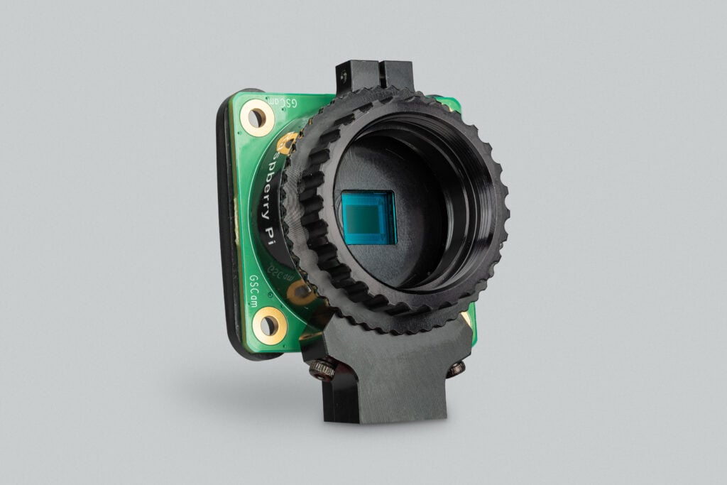
One of the most exciting developments in camera sensor technology comes from STMicroelectronics. At Embedded World 2026, the company unveiled its Vx1943 family of 5MP RGB IR image sensors—CMOS sensors that bring onto a single chip capabilities that traditionally required multiple components.
The breakthrough lies in the hybrid shutter design. Every CMOS designer knows the classic shutter trade-off. With a rolling shutter, exposure progresses line by line across the array. Pixels stay simple, sensitivity and noise performance are strong, and HDR implementation is relatively straightforward. The downside is that fast motion or flickering light causes skew and “jello” artifacts because different parts of the frame are captured at different times.
A global shutter does the opposite: all pixels integrate over the same time window, then transfer charge into in-pixel storage before readout, preserving geometry and synchronizing cleanly with strobed or flickering illumination. The price is extra circuitry and some loss in sensitivity or dynamic range.
Until now, engineers had to pick one behavior early in the design and shape optics, illumination, and processing around that essentially immutable choice. The Vx1943 sensors challenge this trade-off at the pixel level. Shutter mode is no longer a one-time choice in silicon but a parameter that can be changed at runtime.
Inside a 2.25µm pixel, ST has implemented a hybrid structure that operates either as a true global shutter or as a high-performance rolling shutter, with the mode selected via registers on a frame-by-frame basis. For system designers, shutter behavior becomes part of the control loop instead of a fixed constraint.
This dual-mode capability is achieved without increasing die size or sacrificing fill factor, making it well-suited to compact, high-resolution embedded and industrial designs. It represents a fundamental shift in how we think about camera sensor technology.
Breakthrough #4: LOFIC Sensors and the 100 dB Dynamic Range Revolution
Perhaps the most significant breakthrough in camera sensor technology for 2026 is the arrival of LOFIC (Lateral Overflow Integration Capacitor) sensors in the consumer market.
Sony’s LYTIA L910 is a 50-megapixel stacked CMOS sensor that promises to fundamentally change how mobile cameras handle extreme lighting conditions. It is the first model in the LYTIA family to feature the LOFIC structure.
What makes LOFIC so revolutionary? A traditional image sensor wastes excess photovoltaic charge from each photodiode—it simply overflows and is lost. A LOFIC sensor’s transformative improvement is to preserve that excess charge and utilize it in a parallel circuit, creating extra space for electricity and expanding the sensor’s light-gathering capacity.
The results are stunning. The LYTIA L910 can achieve a dynamic range of 100 dB with a single exposure—roughly 16.6 stops. To put that in perspective, that is nearly 17 stops of dynamic range in a smartphone sensor.
Sony combines the LOFIC structure with its new Triple Conversion Gain HDR (TCG-HDR) technology, which reads image data from a single exposure at three different conversion gain levels. Unlike multi-exposure HDR approaches, the single-exposure method minimizes motion blur and light flicker artifacts.
The sensor also incorporates Ultra High Conversion Gain technology, which improves the efficiency of converting light into electrical signals. According to Sony, random noise is reduced by approximately 30% compared to previous solutions, significantly improving image quality in low-light and night photography scenarios.
The LYTIA L910 supports 4K HDR video recording at 60 frames per second while maintaining low power consumption. Sony has announced that mass production shipments are expected to begin during summer 2026, with the first smartphones featuring the new sensor reaching the market in late 2026 or early 2027.
Don’t Forget Check This One:
7 Game-Changing Astrophotography Cameras That Capture Deep Space in 2026
Breakthrough #5: Advanced Autofocus and the RB2×2 OCL Pixel Structure
Autofocus performance has long been a differentiator between good and great cameras. Sony’s LYTIA 610, a 64-megapixel stacked CMOS sensor, introduces the RB2×2 On-Chip Lens (OCL) technology—making it the first image sensor using this pixel structure to enter mass production.
The RB2×2 OCL pixel structure integrates different lens arrangements within a Quad Bayer color filter pattern, enabling the sensor to balance high-resolution image capture with effective phase-detection autofocus performance. The sensor also incorporates a dedicated remosaicing algorithm designed specifically for the new pixel arrangement, reconstructing image data more efficiently and resulting in improved image sharpness and detail.
Sony claims the new sensor delivers a 20% increase in spatial resolution compared with its previous sensor featuring the same pixel size. This improvement is expected to benefit smartphone telephoto cameras, which often face challenges in maintaining image quality while operating within limited space constraints.
Beyond still photography, the LYTIA 610 has been designed to enhance mobile video performance. Improvements in logic circuitry and analog-to-digital conversion technology have doubled the sensor’s readout speed compared with earlier 1/2-inch sensors. The faster processing capability allows support for 4K video recording at 120 frames per second—a feature Sony says is being introduced for the first time in a sensor of this size.
Breakthrough #6: On-Chip RGB-IR Intelligence for Multispectral Imaging
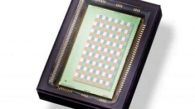
Multispectral imaging—capturing both visible and infrared light—has traditionally required complex external processing. The Vx1943 sensors from STMicroelectronics change this by performing key processing steps directly on the chip.
Using a 4×4 RGB-IR color filter array with dedicated NIR pixels, the sensors execute RGB-IR separation on the logic layer. Instead of delivering a mixed mosaic, the sensor itself splits visible and NIR information. During this step, it performs “RGB cleaning” by estimating the NIR contribution seen by the R (and partly G) pixels from neighboring pure IR samples, subtracting that IR component, and reorganizing the corrected data into a standard RGB Bayer pattern.
The result is an IR-corrected color stream that feeds conventional ISPs with far fewer color shifts under IR-rich lighting and less reliance on aggressive IR cut optics. In parallel, a dedicated NIR pipeline runs ST’s patented Smart Upscale algorithm, fusing measurements from the dedicated IR pixels with the IR content present in RGB sites to reconstruct a full-resolution 5MP NIR image.
Because this operates on the raw RGB-IR mosaic on the 40nm logic layer—before any generic demosaicing or resampling—the sensor preserves edges and fine structures, delivering up to roughly twice the perceived NIR sharpness compared to simple host-side interpolation.
This advancement in camera sensor technology opens new possibilities for security cameras, automotive vision systems, and any application where seeing beyond visible light matters.
Breakthrough #7: The Path to Full-Frame Video in Smartphones
Despite major gains in photo quality, capturing full-resolution video remains challenging due to power, heat, and data throughput limits. Manufacturers are using stacked die architectures to optimize pixel drive and readout, reducing latency and boosting efficiency.
The premium sensor segment is accelerating growth through 2026 as mobile, automotive, and emerging markets adopt AI-enabled, high-performance sensors. Technologies such as 200MP+ resolution, stacked pixels, and advanced HDR are setting new standards for image quality.
Sony’s LYTIA 610, with its ability to record 4K video at 120 frames per second, represents a significant step toward this goal. The sensor also supports 4K HDR video recording at 60 frames per second, helping users capture scenes with significant variations in brightness and contrast.
With smartphone manufacturers increasingly focusing on delivering a seamless multi-camera experience, sensors like the LYTIA 610 can help reduce differences in image quality between primary and telephoto cameras. The combination of high resolution, autofocus precision, and video capabilities is intended to support next-generation mobile imaging systems.
What This Means for Your Photography
The evolution of camera sensor technology in 2026 is not just about technical specifications—it is about what these advancements enable you to do.
Better low-light photography means you can capture stunning images in challenging conditions without a flash. Wider dynamic range means both shadow details and bright highlights are preserved in the same image. Faster readout speeds mean smoother video and less rolling shutter distortion. Smarter autofocus means you never miss the moment.
Whether you are choosing a new smartphone, upgrading your camera, or simply appreciating the technology behind your images, understanding camera sensor technology helps you make informed decisions.
The global image sensor market is expected to reach $68.7 billion by 2034. This growth reflects not just consumer demand but the increasing integration of sensors into every aspect of our lives—from smartphones and automobiles to healthcare and industrial automation.
Enjoy This Article So Far? Don’t Forget Check This One:
From Celluloid to AI: 7 Ways Film Technology Revolutionized Cinema
The Road Ahead
As we look toward the future, several trends will continue to shape camera sensor technology:
AI Integration: Sensors are becoming intelligent, processing data on-chip rather than relying on external processors. This reduces latency and power consumption while enabling new capabilities.
Stacked Architectures: By stacking pixel and logic wafers, manufacturers can pack more functionality into smaller spaces, enabling higher resolution and better performance in compact devices.
New Materials: Innovations in backside structures, photodiode confinement, and light-guiding materials are enhancing color accuracy and reducing noise across large arrays.
Expanded Applications: Beyond photography, sensors are finding new roles in driver monitoring, wearables, robotics, and healthcare.
The shift from pixel scaling to pixel intelligence represents a fundamental change in how we think about camera sensor technology. The race for more megapixels is over. The race for smarter pixels has just begun.
Conclusion
Camera sensor technology in 2026 is more advanced, more capable, and more intelligent than ever before. From hybrid shutters that adapt to any scene to LOFIC sensors that capture nearly 17 stops of dynamic range, the breakthroughs we have explored represent a new era in imaging.
Whether you are a professional photographer pushing the boundaries of creative expression or a smartphone user capturing everyday moments, these advancements in sensor technology are making better images more accessible to everyone.
The next time you take a photograph, take a moment to appreciate the remarkable technology behind it—the tiny silicon chip that turns light into memory, engineering into art, and moments into eternity.